A view to a battery current sensor - shunt or Hall
By Wouter Reusen, Applications Engineer at Melexis
Abstract — Traditionally, shunt-based current sensors have been the preferred choice in many applications due to their inherent accuracy, operating on Ohm’s Law by measuring voltage drop across a known low-resistance shunt resistor. However, this whitepaper demonstrates that advancements in Hall-based current sensing technology, coupled with sophisticated compensation techniques, are challenging this preference. Both shunt- and Hall-based methods can achieve similarly high levels of accuracy, specifically less than 0.5% error, through appropriate compensation strategies. The optimal choice between the two is a nuanced decision, driven by a thorough evaluation of the application’s unique needs regarding galvanic isolation, total system cost, and the practicalities of calibration and compensation.
1. Introduction
Battery pack current measurements are essential in Hybrid Electric Vehicles (HEV) and Electric Vehicles (EV). It is important to prevent batteries from operating outside of their safe limits by shutting down the system when these limits are exceeded, preventing potentially dangerous overcurrents or short circuit events.
Besides these safety functions, the battery pack current is also used to estimate the battery’s State of Charge (SOC), State of Health (SOH) and State of Power (SOP). A battery can be used more efficiently when the SOC, SOH and SOP parameters are estimated more precisely, allowing the range and lifetime of a battery to be extended, while permitting more compact designs which lowers system cost. Finally, monitoring the current precisely during charging can enhance the charging process, resulting in faster charging sessions.
Shunt-based current sensing methods are considered the mainstream method for current measurements in today’s architecture for Battery Management Systems (BMS), as shown in Figure 1. Hall-based current sensing methods are often used as a redundant current measurement in order to achieve a higher automotive safety integrity level (ASIL) and the posibility to place the Hall-based current sensor on the high side where shunt-based current sensors are typically placed on the low side. The reason for this is that typical shunt-based current sensing methods are considered more accurate than Hall-based current sensing methods.
However, Hall-based current sensing methods are becoming more accurate and are even starting to compete with shunt-based current sensing methods.
This whitepaper provides an objective comparison of shunt- and Hall-based current sensing techniques. Section 2 outlines the fundamental principles of shunt-based sensing, key error sources, and corresponding compensation methods. Section 3 presents the same analysis for Hall-based sensing. Section 4 compares the two approaches, and Section 5 concludes this paper.

Fig. 1. HV BMS architecture.
However, Hall-based current sensing methods are becoming more accurate and are even starting to compete with shunt-based current sensing methods.
This whitepaper provides an objective comparison of shunt- and Hall-based current sensing techniques. Section 2 outlines the fundamental principles of shunt-based sensing, key error sources, and corresponding compensation methods. Section 3 presents the same analysis for Hall-based sensing. Section 4 compares the two approaches, and Section 5 concludes this paper.
2. Shunt-based current sensing
A shunt-based current measurement is probably one of the simplest ways of measuring a current in an electric circuit. A shunt is a very precise resistor with a very low resistance and a current flowing through a circuit can be measured by placing a shunt in series with that circuit. A voltage drop across the shunt resistor occurs when a current flows through the shunt. Ohm’s Law states that the voltage drop across the shunt (Vshunt) is equal to the current through the shunt (Ishunt) times the resistance of the shunt (Rshunt). Hence, the current can be derived by measuring the shunt voltage:
The shunt voltage must be digitized, allowing an embedded system to calculate the current. Before it can be digitized by an analog-to-digital converter (ADC), the shunt voltage must be amplified. An analog front-end (AFE) is typically used to convert and amplify the differential shunt voltage to a single-ended voltage. This is visualized in Figure 2.

Fig. 2. Typical blockdiagram of a shunt-based current measurement.
2.1 Error sources and compensation methods in shunt-based current sensing
The overall accuracy of the shunt-based current measurement depends on the selected AFE, ADC and shunt resistor. In addition, the final precision of the shunt measurement will be influenced by the cables connecting the shunt to the AFE.
2.1.1 Analog Front End (AFE)
The AFE prepares the analog shunt voltage for digitalization. This includes the amplification, compensation and conversion from a differential to a single-ended voltage. Measurement errors of the AFE are mainly due to temperature and lifetime drift of the gain, offset and common mode voltage. Temperature drift errors can be compensated by an end-of-line (EOL) calibration but can be rather expensive to compensate for, while lifetime drift errors cannot be compensated for.
2.1.2 Analog-to-Digital Converter (ADC)
The amplified and compensated single-ended voltage of the AFE is converted to a digital value using an ADC. The relationship between the analog and digital values is represented by a transfer function. This transfer function may suffer from gain, offset and linearity errors and can also drift over temperature and lifetime.
The transfer function of an ADC looks like a staircase, where the height of a step represents the resolution of the ADC. The resolution of the ADC is expressed in bits and defines the smallest detectable change in the analog signal, with higher resolution allowing for smaller changes in the analog signal to be detected. The quantization error is directly linked to the resolution of the ADC and is defined as the difference between the original analog value and the digitized value. This can also result in quantization noise.
The full-scale range of the ADC (the height of the staircase) is established by a reference voltage. The input voltage is compared with the reference voltage in order to determine its digital equivalent. This means that variations in the reference voltage cause variations in the digital signal.
Offset, gain, linearity and noise errors can be easily compensated for by software. On the contrary, errors due to quantization and unstable reference voltages are hard to compensate for.
2.1.3 Shunt
High-power precision resistors usually consist of two terminals and the actual shunt resistor. The terminals are made of copper and are welded to the shunt resistor, which is usually an alloy of copper and manganese. The copper-manganese alloy has the property of being very temperature stable but has a higher resistance than copper. Shunt resistors can have some significant inaccuracies. These inaccuracies are mainly caused by Joule heating, and they imply a change in the resistance and/or a generation of an electromotive force (EMF) voltage. Aging of the shunt resistor will also degrade the accuracy and is caused by different environmental factors, like temperature, humidity, vibration, mechanical stress, etc.
The manufacturing process affects the actual resistance of the shunt resistor. The variation in resistance is expressed as a percentage of the nominal resistance. The tolerance of a shunt acts as an offset in resistance at room temperature (e.g. 20°C) and is given by:
The actual resistance can be measured by forcing a known current through the shunt and by measuring the voltage drop across the shunt. It is important to keep the shunt resistor at room temperature, because the shunt resistance varies over temperature. The variation of resistance over temperature is given by the temperature coefficient of resistance (TCR). An example of the variation of the resistance of a copper-manganese alloy is shown in Figure 3 with a dark blue line. The solid line represents the nominal resistance variation over temperature, while the dashed lines represents the minimum and maximum resistance variation over temperature.

Fig. 3. Resistance variation over temperature.
The resistance variation over temperature of a copper-manganese alloy can be approached by a second-order function:
where T is the temperature of the shunt and c0, c1 and c2 are the coefficients of the second-order function.
As a result, the resistance of the shunt at a given temperature (R@T) can be estimated as follows:
Some shunt manufacturers provide the actual resistance and the coefficients of the second order function in the form of a data matrix code (DMC). However, if the DMC is not available, part-to-part calibration can be performed. At least three temperatures must be applied to get a good approximation of the second-order function. Changing the temperature is a rather slow process and can be too expensive, particularly when the thermal mass of the sensor module or lower resistivity shunt gets bigger. Therefore, it can be more beneficial to perform the calibration only at room temperature and to use the typical copper-manganese TCR for compensating the resistance variation over temperature, at the expense of accuracy loss. This is referred to as ’blind calibration’ in this whitepaper. The expected error after blind calibration is visualized in Figure 4 with the dark blue dashed lines.

Fig. 4. Error after blind calibration.
Fairly simple compensation methods for the actual resistance and the resistance variation over temperature have been discussed up to now. Since it is not possible to make the connection between the AFE and the shunt resistance directly on the copper-manganese alloy, it must be done on the copper terminals instead. The influence of the extra resistance of the terminals has not been considerd so far. It is well known that copper has a low resistivity, but a high TCR, and the high TCR of copper may induce some significant errors.
Assume that 2.5mm of copper on both sides of the terminals contributes to the total resistance measured by the AFE and that the width and thickness of the terminals is 18mm and 3mm, respectively. See Figure 5 for the equivalent schematic of the total resistance of the shunt resistor. Knowing that the resistivity of copper at 20°C is about 1.7μΩ.cm, the resulting resistance of the copper in one terminal (Rterminal) is:

Fig. 5. Equivalent schematic of the total resistance of the shunt resistor.
Where ρ is the resistivity of copper at 20°C, l is the length of the copper and A is the cross-sectional area of the copper.
Shunt resistors of 100μΩ are no exception nowadays. This leads to a total resistance of 101.574μ Ω seen by the AFE. The variation in the total resistance over temperature, using a TCR of 3900ppm/K for copper and the previously used variation over temperature of a copper-manganese alloy, is shown in Figure 3 with a green line.
The resulting error after blind calibration, using the nominal TCR of the copper-manganese alloy is shown in Figure 4 with the green dashed lines. A temperature calibration after assembly can be perfomed to reduce the influence of the additional copper resistance or the standard shunt can be replaced by a shunt with holes/slits next to the connection points of the AFE. This is a patented technique [2] [3] [10] known as ’current shadowing’.
Another source of inaccuracy, which mainly contributes to the offset error, is the generation of an EMF voltage. When two dissimilar metals are connected together at both ends, forming two junctions, a thermocouple is created. This thermocouple develops an EMF voltage when both junctions are maintained at different temperatures. The relationship between the generated EMF voltage (ΔV) and the temperature difference (ΔT) is described by the overall Seebeck coefficient (S):
For example, an overall Seebeck coefficient of 1μV/K is given for a combination of copper and a copper-manganese alloy, and the maximum expected temperature difference between the two junctions is 10°C. This leads to a generated EMF voltage of 10μV, resulting in an input-referred offset error of 10mA when using the same shunt of 100μΩ. This thermo-electric effect increases linearly with decreasing shunt resistance, making this effect more dominant with low-ohmic shunts for high current applications. The length of the copper-manganese alloy is reduced to decrease the resistance of the shunt. At some point, the length cannot be reduced anymore and thus the width of the shunt is increased. Shunts with a resistance of 25μΩ and lower have a typical width of 36mm. The cost, size and weight for these types of shunts are increased because the amount of material is increased.
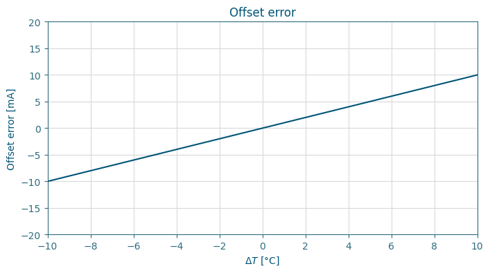
Fig. 6. Offset error.
The unwanted EMF voltage can be actively compensated by measuring the junction temperatures of the shunt resistor. However, it is very difficult to measure the actual core temperature of the material at the position of the junctions, so it is better to reduce the effect by minimizing the temperature gradient over the shunt. This can be achieved by making the design as symmetrical as possible [9].
Finally, there is the lifetime drift of the shunt resistor, caused by material degradation, temperature cycling, contamination, and other effects. It is required to recalibrate the shunt-based current sensor; otherwise, the lifetime drift can reach up to 1%. Recalibration during usage in the field is rarely possible as it requires an accurate reference current to be generated on site. The lifetime drift error is often overlooked during the selection phase of the current sensing method and they should be added to the total error budget of the shunt-based current sensing method.
2.1.4 Wiring
The AFE has a high impedant differential input. The matching of these two input impedances, especially over temperature, also plays a role in the error budget. A small amount of current flows through the wires connecting the shunt to the AFE and the AFE itself. This leakage current causes a voltage drop across the connecting wires, which is added to the total measured voltage. The wires can also act as an antenna and pick up some noise in electromagnetic environments. Both the leakage current and the noise lead to additional errors. Figure 7 visualises the accuracy of current measurements when using different types of shunts. The lowest accuracy is obtained with a type 1 shunt and long wires. Type 1 shunts do not contain temperature sensors and DMCs for temperature compensation, and the long wires can pick up unwanted noise. Using shorter wires and a type 2 shunt increases the accuracy of the measurement system. Type 2 shunts contain temperature sensors and DMCs for temperature compensation. However, the signal is still an analog signal. Type 3 shunts, better known as smart shunts, are being introduced to improve accuracy and reduce the load on the central processing unit (CPU). All compensation calculations can be performed on the smart shunt instead of on the CPU. They can operate in environments with high levels of electromagnetic energy since the wires connecting the shunt and the AFE are very short and thanks to a robust digital communication protocol for electromagnetic interference (EMI).

Fig. 7. Shunt accuracy versus shunt intelligence.
3. Hall-based current sensing
When a current flows through a conductor, a magnetic field is generated around the conductor. The magnetic field strength decreases when moving further from the center of the current conductor. The current through the conductor (I) can be derived by measuring the magnetic flux density (B) at a distance from the conductor (r):
where μ0 is the permeability of a vacuum.
Stray fields will influence the magnetic field measurements, causing wrong estimations of the current. Traditionally, a ferromagnetic core is placed around the current conductor to improve the so-called stray field immunity (SFI) as well as to increase the signal by concentrating the magnetic field. The magnetic flux density (B) is measured inside the air gap of the ferromagnetic core with length (Lair), and the current (I) can be derived using the following formula.
Where Lcore is the path length in the core, μcore is the permeability of the core material and μair is the permeability of the air. Formula 8 can be rewritten as follows:
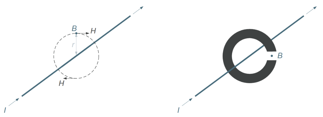
Fig. 8. Typical blockdiagram of a Hall-based current measurement.
Hall-effect sensors are used to measure the magnetic flux in the air gap of the ferromagnetic core. The output of such a Hall-effect sensor is typically a voltage which has a linear relation with the applied magnetic flux. The output voltage range is typically 0-5V or 0-3.3V and can be digitized with an ADC.
3.1 Error sources and compensation methods in Hall-based current sensing
The overall accuracy of the hall-based current measurement depends on the selected Hall-effect sensor, ADC and ferromagnetic core. As the ADC has already been discussed in the previous section, it will not be covered in this section.
3.1.1 Hall-effect sensor
Hall-effect sensors provide an analog output voltage proportional to the applied magnetic flux density. The transfer characteristics of these sensors are factory calibrated for temperature, and the manufacturer guarantees that these characteristics fall within predefined ranges. This results in measurement errors, which can be categorized into three groups: sensitivity errors, offset errors and non-linearity errors.
The sensitivity error is proportional to the input current and includes:
- Sensitivity programming resolution (S)
- Thermal sensitivity drift (ΔTS)
- Lifetime sensitivity drift (ΔLS)
- Ratiometric sensitivity error (ΔRS)
- Non-linearity error (NLE)
The offset error includes:
- Quiescent output voltage (VOQ)
- Thermal offset drift (ΔTVOQ)
- Lifetime offset drift (ΔLVOQ)
- Ratiometric offset error (ΔRVOQ)
- Noise (N)
All the errors except the lifetime drift errors can be compensated during EOL calibration. As is the case for shunt, temperature drift errors are expensive to compensate for at module level, which is why they are conducted at IC level by the sensor supplier.
3.1.2 Ferromagnetic core
The field factor (FF) describes the relationship between the applied current (I) and the measured magnetic field (B) inside the air gap of a ferromagnetic core. It depends on the permeability of air, the path length in the air, the permeability of the ferromagnetic material and the path length in the ferromagnetic material. The position of the Hall-effect sensor inside the air gap also affects the field factor, despite the predominantly homogeneous field in the air gap. On top of this, all ferromagnetic materials suffer from hysteresis, which induces an extra source of error.
Both the production of the ferromagnetic core and the assembly of the Hall-effect based current sensing module involve mechanical tolerances. This results in an offset error of the field factor. The offset error is dominated by the path length in the air and the position of the sensor inside the air gap.
The actual field factor can be measured by forcing a known current through the conductor and by measuring the magnetic flux in the air gap with the Hall-effect sensor. Unfortunately, the field factor will not be the same for different applied currents. This is because the relative permeability of a ferromagnetic material is not a constant value; it changes with applied magnetic field strengths. This results in a non-linear relationship between the applied magnetic field and the measured magnetic flux density in the air gap. This effect is visualized in Figure 9

Fig. 9. BH - BM curve.
Ferromagnetic cores used in Hall-based current measurements can come with different structures, materials, shapes, and other physical characteristics. The most commonly used structures are laminated and wound cores. Cores are laminated to reduce the effect of Eddy currents, which improves the frequency response. The improvement of the frequency response is out of scope and will not be discussed in this whitepaper, since the battery pack currents are mainly DC.
Laminated cores are more cost-effective to manufacture than wound cores, which require more complex manufacturing processes. However, since wound cores are inherently grain oriented, they have less hysteresis compared to laminated cores. The hysteresis does not only depend on the structure of the core but also on the material used. Silicon ferrite (SiFe) and nickel ferrite (NiFe) are the most common used materials, where NiFe has a lower hysteresis, but a significantly higher price tag compared to SiFe.
Hysteresis in magnetics is defined as the lag of magnetic flux density (B) to an applied magnetic field (H). This is visualized in the BH-curve (Figure 10) and described as follows. The origin of the BH-curve (0) states that the ferromagnetic material is fully demagnetized, meaning that the magnetic flux density (B) is 0 mT when a magnetic field (H) of 0 A/m is applied. B increases when H increases and follows the initial magnetization curve until saturation is reached. The initial magnetization curve is the line between (0) and (1). When H is decreasing, B is also decreasing, but it does not follow the initial magnetization curve anymore. When the applied magnetic field is removed (2), the ferromagnetic material still retains some amount of magnetism; this is called the remanence (Br). The magnetic field needed to fully remove the remanence (3) is called the coercivity (Hc). B further decreases when H decreases until negative saturation is reached (4). The sequence from (1) to (4) is repeated for increasing H and B to close the hysteresis loop. The amount of remanence depends on the history, which is the previously applied magnetic field intensity. Different hysteresis loops are visualized for different histories of applied magnetic fields in Figure 11.
To curb this accuracy impact at low currents, dual-range current sensing solutions have been developed, exploiting the advantages of NiFe for the small range and SiFe for the large range. A SiFe ferromagnetic core is used for the full-scale current range, together with a Hall-effect sensor optimized for this range. A NiFe ferromagnetic core, with lower hysteresis, is used for the small range together with another Hall-effect sensor optimized for this range.
However, dual-range current sensors are rather bulky and expensive. A more cost-effective solution would be to develop a hysteresis compensation algorithm on a microcontroller, but this requires a very accurate Hall-effect sensor with a low offset and gain error.
The material properties of the ferromagnetic core depend on the temperature, meaning that the BH-curve changes over temperature. Typically, the BH-curve becomes narrower and less steep as the temperature increases and finally disappears once it reaches the Curie temperature. The BH-curve does not only change over temperature but also over lifetime due to magnetic aging, mechanical stress, material degradation, etc. It is important to choose performance ferromagnetic cores made of high-quality material with state-of-the-art processing control, such as heat and surface treatments.
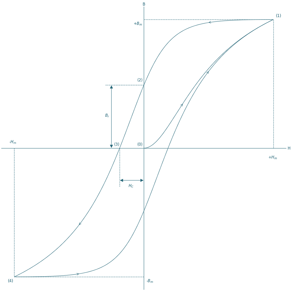
Fig. 10. BH curve.
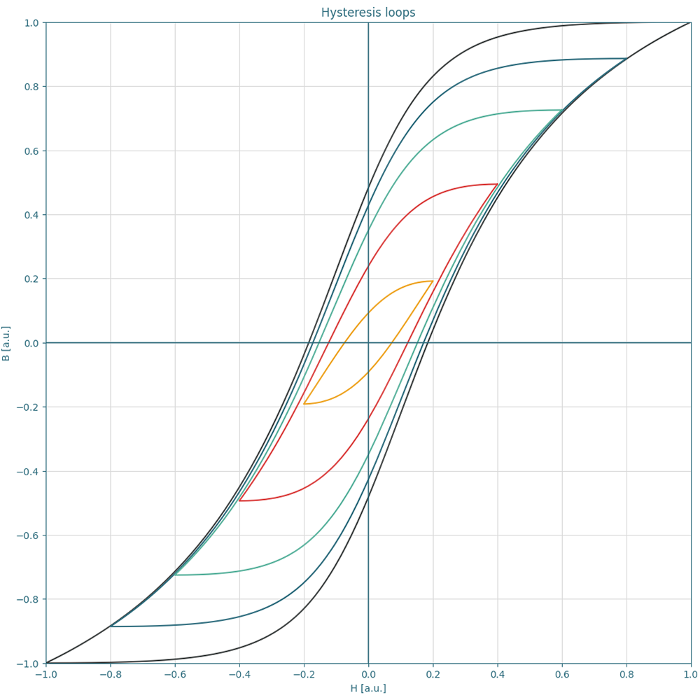
Fig. 11. Hysteresis loops.
4. Experimental results
4.1 Shunt-based current sensing
The shunt-based current sensing module used in this experiment comprises a MLX91231KGO-BBC-000 [8] smart current/voltage/temperature (IVT) shunt interface current sensor and a VSPA6918SY-0M10J [1] precision shunt resistor. Table 1 summarizes some key features of the shunt interface and the shunt resistor.
Two experiments were conducted to assess the performance of shunt-based current sensing. The first experiment focused on the bare shunt’s performance, while the second evaluated the complete shunt-based current sensing module.
Table 1
DVK91231 REV2.0 [6] specifications
| Component | Characteristics | Value |
| VSPA6918SY-0M10J | Resistance value | 100μΩ |
| Resistance tolerance | ±5% | |
| TCR | ±100ppm/K | |
| Thermal EMF | < 3μV/K | |
| MLX91231KGO-BBC-000 | Sensitivity thermal & lifetime drift | ±0.25% |
| Offset thermal & lifetime drift | ±1μV |
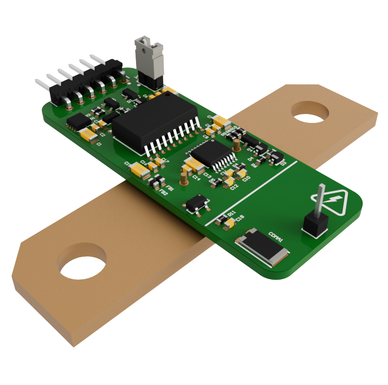
Fig. 12. DVK91231 REV2.0.
In both experiments, the shunt-based current sensing module is placed in a climate chamber to change the temperature. A high-powered DC power supply is used to force a current through the shunt, while a high-accuracy current probe operating at room temperature is used as a reference.
4.1.1 Bare shunt performance
The MLX91231KGO-BBC-000 voltage output and the high-accuracy current probe output are used to determine the shunt resistance at various temperatures. Monitoring the temperature of the shunt resistance is done via the MLX91231KGO-BBC-000’s negative tempeature coefficient (NTC) temperature sensing function. The measured variation of the shunt resistance is plotted as the yellow line on top of the theoretically calculated variation of the shunt resistance in Figure 13. There is a good match between the experimental and the theoretical values. Note that these results represent the variation of the shunt resistance (copper-manganese alloy) together with the extra resistance of the terminals (copper).

Fig. 13. Measured resistance variation of the total shunt resistance (Cu-Mn alloy + Cu terminals).
Typically, 5mm of copper with a cross-sectional area of 0.54cm2 contributes to the total resistance measured by the MLX91231KGO-BBC-000. This results in an extra 1.574μΩ resistance at room temperature. A TCR of 3900ppm/°C is used to estimate the extra resistance of the copper terminals for different temperatures. This extra resistance is then subtracted from the measured resistance and is plotted as the red line on top of the theoretically calculated variation of the shunt resistance in Figure 13.
Note that these results represent the variation of the shunt resistance (copper-manganese alloy) alone. In order to verify the mathematical compensation, two holes were drilled next to the press fit pins of the shunt to mimic the patented principle of current shadowing. The full experiment is then repeated, and the results are plotted as the green line in Figure 14. This shows a good match between the theoretical values and both experimental values.

Fig. 14. Measured resistance variation of the total shunt resistance (Cu-
Mn alloy).
Both the VSPA6918SY-0M10J and the MLX91231KGO-BBC-000 were placed in the climate chamber during the previous experiment. The MLX91231KGO-BBC-000 performs excellently at different temperatures, as the theoretical calculations of the shunt’s TCR correspond to the experimental results. All of the above results prove that the MLX91231KGO-BBC-000 can be used for the next experiment.
4.1.2 Shunt-based current sensing module performance
Section 2.1.3 detailed the error sources of the shunt resistor, and these were subsequently verified through measurements in the preceding section. This section details various compensation methods and analyzes their performance.
The simplest compensation method is the gain and offset calibration. For a shunt-based current sensor, this is expressed as:
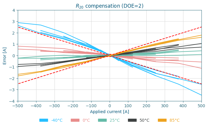
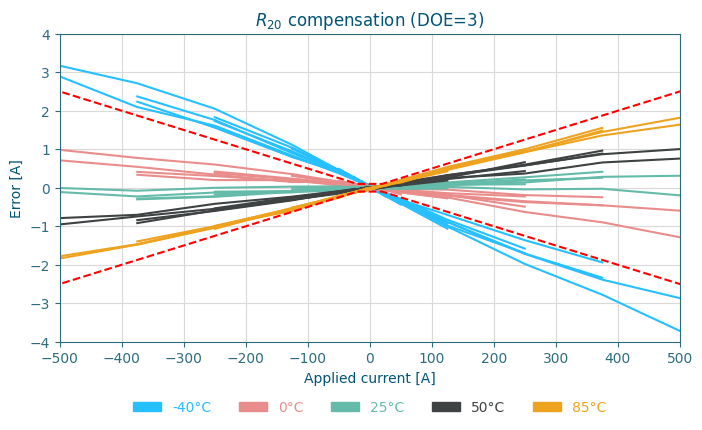
The shunt resistance (Rshunt) is measured at room temperature and is denoted as (R20), hence the (R20) compensation. The current measurement error of three design of experiment (DOE) devices for five different temperatures after the (R20) compensation is shown in Figure 15.

(a)
(b)
(c)
Fig. 15. Current measurement error after R20 compensation for 3 shunt-based current sensing DOEs.
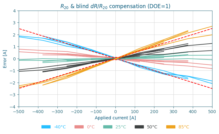
More advanced compensations can be completed if the temperature of the shunt is available. The change of the resistance of the copper-manganese alloy over temperature is usually described in the datasheet of the shunt, and thus it can be estimated using the shunt temperature measurement. Rshunt in the previous formula can be replaced by the estimated resistance of the copper-manganese alloy at a given temperature (RCuMn@T) in order to calculate the current.
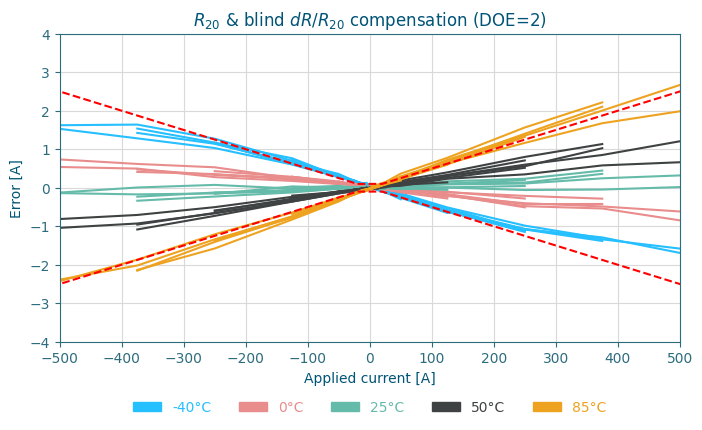
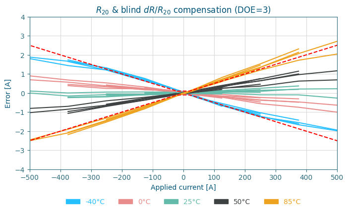
This compensation method is referred to as the R20 & blind ΔR/R20 compensation. The current measurement error of three DOE devices for five different temperatures after the R20 & blind ΔR/R20 compensation is shown in Figure 16.
(a)
(b)
(c)
Fig. 16. Current measurement error after R20 & blind ΔR/R20 compensation for 3 shunt-based current sensing DOEs.
Significant errors persist even after R20 & blind ΔR/R20 compensation. These errors stem from the additional copper material situated between the copper-manganese alloy and the shunt voltage measurement terminals. It is feasible to estimate the extra resistance of the copper material, but this should be done carefully. The resistance of the copper can vary between different shunt resistors due to the mechanical tolerances, but also the TCR of the used copper can vary between different shunt resistors. The extra resistance of the copper in terminals at room temperature (RCu) is estimated as follows:
Therefore, the extra resistance of the copper in terminals at a given temperature (RCu@T) is:
Where (Tshunt) is the temperature of the shunt and (TCRCu) is the TCR of copper.
The total resistance (Rtotal) seen by the MLX91231KGO-BBC-000, and which is used to calculate the current, is:
The current measurement error of three DOE devices for five different temperatures after the R20 & blind ΔR/R20 & Rcu compensation is shown in Figure 17.
All the prior compensations are performed by the MLX91231KGO-BBC-000 thanks to the embedded microcontroller (MCU) and the NTC temperature sensing function.

(a)

(b)

(c)
Fig. 17. Current measurement error after R20 & blind ΔR/R20 & Rcu compensation for 3 shunt-based current sensing DOEs.
4.2 Hall-based current sensing
The Hall-based current sensing module, used in this experiment, comprises a MLX91230KDC-BBC-200 smart [7] contactless current sensor and a SiFe LU-8.6-6-17-5.75 core [4]. The below table summarizes some key features of the contactless current sensor and the ferromagnetic core.
Table 2
DVK91230 REV2.0 [5] specifications
| Component | Characteristics | Value |
| LU-8.6-6-17-5.75 | Field factor | 145.35μT/A |
| Material | SiFe | |
| Saturation | 1.5T | |
| Hysteresis | 100A/m | |
| MLX91230KDC-BBC-200 | Sensitivity thermal drift | ±0.5% |
| Offset thermal drift | ±60μT |
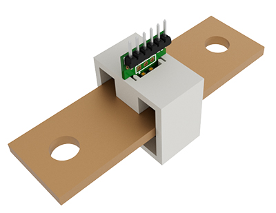
Fig. 18. DVK91230 REV2.0.
4.2.1 Hall-based current sensing module performance
The gain and offset calibration is also the simplest calibration method for Hall-based current sensors. The transfer function is as follows:
However, the effect of the magnetic hysteresis is clearly visible. Figure 19 shows the current measurement error of three DOE devices for five different temperatures after the gain and offset calibration.
(a)

(b)

(c)
Fig. 19. Current measurement error after gain and offset calibration for 3 Hall-based current sensing DOEs.
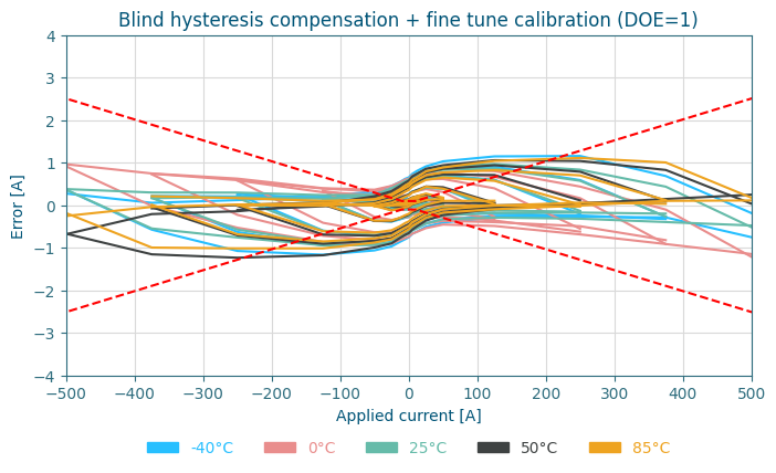
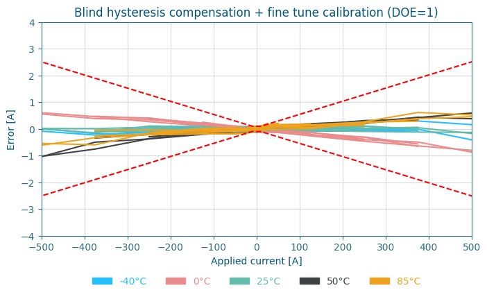
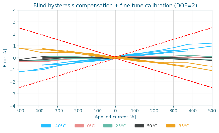
Advanced algorithms can compensate for the magnetic hysteresis. A blind hysteresis compensation model, developed for this experiment and called TruFlux™, processes the measured magnetic field to produce a hysteresis-free output. TruFlux™ is a generic model that is able to run on different Hall-based current sensors of the same type, without the need to update parameters. The NLE of the ferromagnetic core is not yet compensated, but fortnately these compensation parameters are repeatable and can also be shared between different Hall-based current sensors of the same type. 5 The TruFlux™ and NLE model will compensate for the hystersis and non-linearity of the core, but not for the mechanical tolerances and the variations between the MLX91230KDC-BBC-200. A gain and offset calibration at room temperature is still needed to remove the variablity between the Hall-based current sensors of the same type. The current measurement error of three DOE devices for five different temperatures after compensation using the TruFlux™ and NLE model in combination with a gain and offset calibration is shown in Figure 20
(a)
(b)

(c)
Fig. 20. Current measurement error after TruFlux™ compensation, NLE compensation and gain and offset calibration for 3 Hall-based current sensing DOEs.
5. Shunt versus Hall
The MLX91231 and MLX91230 utilize identical analog and digital circuitry, enabling an equitable comparison between shunt- and Hall-based current sensing methodologies. This comparison encompasses the entire system rather than just the interface IC — a common oversight when selecting a current sensor.
The bare shunt exhibits a relatively large temperature drift compared to the bare ferromagnetic core. This translates into gain errors. The ferromagnetic core, on the other hand, suffers from magnetic hysteresis that depends on the history of the applied magnetic field. This results in a non-linear behavior and significant offset errors. The experiments show that both shunt-based and Hall-based current sensors require some compensation to achieve an accuracy of less than 0.5%.
Calibrating Hall-based current sensors is slightly more complex than calibrating shunt-based sensors. However, the initial measurement to determine compensation parameters for the blind hysteresis model only need to be performed once per core lot. Subsequent gain and offset calibration of Hall-based sensors is comparable in complexity to that of shunt-based sensors.
High-volume market forces are driving the quest for the good-enough-performance at the lowest Total Cost of Ownership (TCO). This price performance elasticity was at the basis of the development of the TruFlux™ algorithm to offer an alternative to shunt-based current sensing solutions. The comparison of current sensing technologies shows that the Shunt-based sensor sets the benchmark with an accuracy of 0.3% at the reference price. The Hall-based sensor emerges as the most attractive option for balancing performance and cost, as it achieves the same high accuracy of 0.3% while being significantly cheaper, with a price 35% lower than the shunt. Conversely, the fluxgate sensor offers the lowest accuracy at 0.5% and is the most expensive of the three, with a cost that is 5% higher than the shunt-based reference.
6. Conclusions
Table 3
Comparison shunt versus Hall
| Hall-based current sensing |
Shunt-based current sensing |
|
| Offset accuracy [mA] | ± 150mA | ± 50mA (100μΩ) ± 100mA (25μΩ) |
| Sensitivity accuracy [%] | 0.3% | 0.3% |
| Isolation | ✓ | ✗ |
| Cost | Low | Medium |
| Complexity | Medium | Easy |
Traditionally, the shunt-based current sensor has been the preferred method, valued for its inherent 0.3% precision, which is derived from a direct measurement using Ohm’s Law. However, the reported instantaneous accuracy of shunt-based current sensing methods often fails to account for practical long-term and environmental stability limitations. A significant factor is the shunt’s lifetime drift, which can degrade the system accuracy by up to 1% over its operational life. Furthermore, the measured voltage critically includes the resistance of the copper terminals, which introduces a notable and highly variable drift due to temperature sensitivity.
Recent advancements in Hall-based current sensing, coupled with the TruFlux™ algorithm, offer a robust solution to these challenges. This whitepaper demonstrates that modern Hall-based current sensors can achieve an instantaneous accuracy of 0.3%, matching that of the shunt. Importantly, the Hall-based approach provides galvanic isolation lowering the total cost of the current sensor module.
In conclusion, while shunt-based current sensors offer high initial precision, their system-level viability is compromised by 1% lifetime drift and temperature-dependent terminal resistance drift, leading to a total error of 1.3%. TruFlux™ presents a compelling alternative, offering equivalent instantaneous accuracy, and a substantial cost advantage, achieving a price reduction of 35% compared to shunt-based solutions. The selection criteria should, therefore, prioritize the sensor’s total lifetime error budget, stability across the operational temperature range, and the benefits of galvanic isolation over traditional reliance on the shunt AFE specifications alone.
References
- CYNPW-21Z-007. VSPA6918SY-0M10. Version A1. Cytec. Sept. 2025.
- Tzu-Hao Hung and Ying-Da Luo. Resistor having low temperature coefficient of resistance. 2020.
- Benedikt Kramm, Felix Lebeau, and Jan Sattler. Current-sensing resistor. 2021.
- LU-8.6-6-17-5.75. F-CR-241-R0. Version R0. PML. Oct. 2025.
- Melexis. Development kit for the smart MLX91230. /en/product/dvk91230-rev2. 2025.
- Melexis. Development kit for the smart MLX91231. /en/product/dvk91231-rev2. 2025.
- Melexis. Smart IVT current sensor ±0.5% accuracy over temperature. /en/product/MLX91230/Smart-IVT-Conventional-Hall-Current-Sensor . 2023.
- Melexis. Smart IVT shunt interface current sensor. /en/product/MLX91231/Smart-IVT-Shunt-Interface-Current-Sensor . 2023.
- Elisa Rodriguez de la Rosa. Master thesis: Analysis of the thermoelectric effect impacting the error of high-precision shunt-based current sensors for high DC current. 2023.
- Todd Wyatt et al. Resistors, current sense resistors, battery shunts, shunt resistors, and methods of making. 2023.

