License to Switch
By Billy Ye, Product Line Director at Melexis
Introduction: The Challenge of High-Speed Power
Modern electric vehicles and industrial power systems are driven by a demand for maximum efficiency. To achieve this, power components—particularly wide-bandgap technologies like Silicon Carbide (SiC)—must switch on and off at unprecedented speeds.
However, pushing these high-voltage devices to their limits creates a physical trade-off. High switching speeds (di/dt) inevitably generate destructive noise, manifesting as massive voltage spikes and high-frequency oscillations (ringing). These transients stress main power components, create localized hotspots, and compromise system reliability.
The monolithic snubber acts as a necessary shock absorber, protecting delicate power electronics from these self-generated surges and enabling the next generation of power modules.
The Technical Obstacle: Parasitics and Ringing
The fundamental challenge arises from the interaction between switching speed and stray inductance.
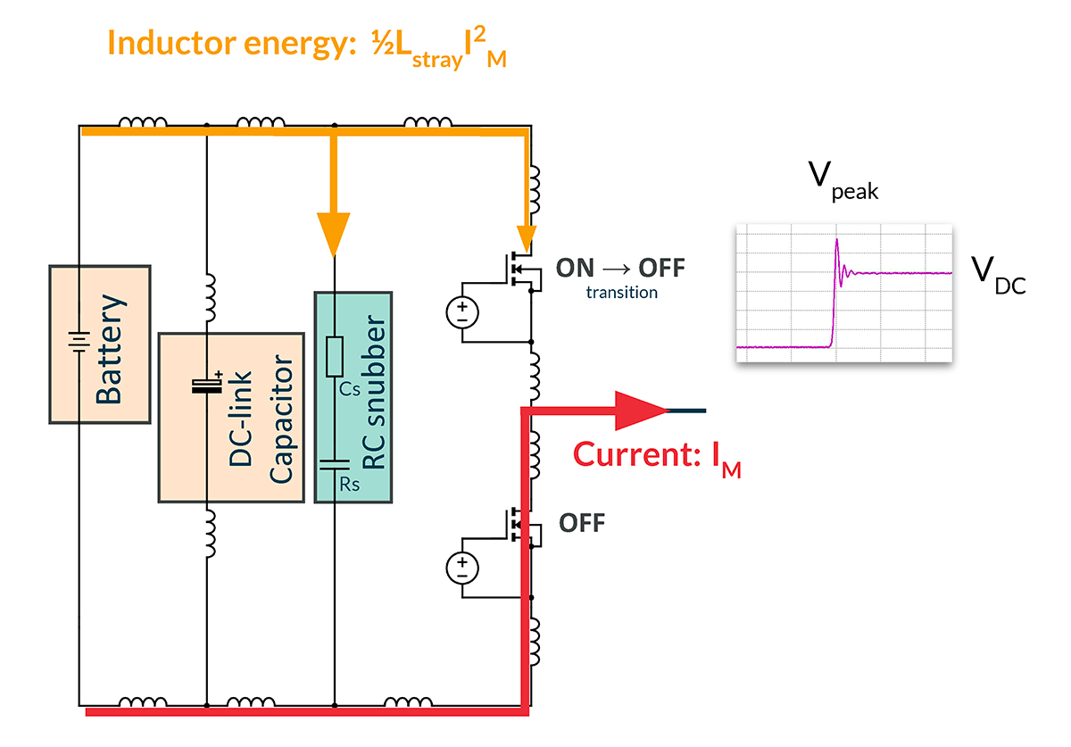
Figure: Schematics - Snubber working principle
1. Voltage Spikes (Vpeak)
Fast switching currents interacting with parasitic inductances (Lstray) inherent in the module layout (busbars, terminals, Direct Copper Bonded DCB traces) generate large voltage peaks according to the formula:
Excessive Vpeak forces engineers to overdesign MOSFETs with higher breakdown voltages to avoid catastrophic failure, often at the cost of performance or price.
2. Parasitic Ringing
The power module circuit, typically a half-bridge topology, forms an inherent RLC resonant circuit during switching events. Since the internal resistance (R) and capacitance (C) are minimal, this circuit is highly underdamped. This results in high-frequency, sustained parasitic ringing that contributes to Electromagnetic Interference (EMI) and power loss.
The Solution: Monolithic High-Voltage Silicon RC Snubber
The MLX91299 introduces a Monolithic High-Voltage Silicon RC Snubber. Unlike bulky discrete ceramic components, which often lack proper thermal dissipation and reliability, this solution integrates the resistance and capacitance components into a single, compact silicon bare die.
Working Principle
The RC snubber resolves the RLC ringing issue by introducing a properly sized Resistor (RS) and Capacitor (CS) into the commutation loop.
- Capacitor Function: The capacitor (CS) stores the inductive energy (½ L IM²) that would otherwise be released destructively as a voltage overshoot. The energy balance requires:
CS > (Lstray × IM²) / (VPeak² - VDC²)
- Resistor Function: The resistor (RS) acts as a dampener, converting the stored energy into manageable heat. For efficient damping (ζ > 0.5), the resistor value must satisfy:
RS > √(Lstray / CS)Furthermore, the snubber is designed to reset quickly enough for the next switching cycle:RS CS ≪ τswitch
Technical Specifications
- Construction: Integrated silicon bare die (Series R and C).
- Voltage Handling: Designed for DC-link applications up to 1000 Vdc (operating) with a peak operating voltage of 1200 Vp. The device features a high Breakdown Voltage (Vbr) of >1500 V.
- Electrical Characteristics: Maintains constant capacitance for voltages above 150 V and exhibits ultra-low leakage current (~ 10-8 A).
- Configurations: Various R and C combinations are available, such as 4.3 nF at 1.45 Ω or 1.1 nF at 5.23 Ω.
System Integration: A Seamless Fit
The MLX91299 is provided as a rectangular silicon bare die, allowing it to be integrated using standard power module manufacturing processes. This "bare die assembly" approach improves long-term reliability by reducing the number of electrical joints compared to discrete solutions.
- Assembly Compatibility: The backside metallization supports both sintering and soldering processes. The top side is designed for wire bonding (e.g., aluminum bonding) for electrical interconnection.
- Thermal Management: Because the snubber is integrated directly alongside SiC components, it leverages the same thermal dissipation channels. This minimizes hotspots and ensures consistent performance even at SiC junction temperatures up to 200°C.
- Topology: The snubber can be implemented as an Output Snubber (parallel with MOSFETs) or a DC-link Snubber (parallel with the DC-link capacitor).
Benefits and Performance
The Silicon RC snubber serves as a "Power Module Booster," delivering the following quantifiable benefits:
| Technical Benefit | Detailed Impact & Quantification |
| Reduction of Switching Losses | By mitigating ringing, the snubber reduces the Eoff (turn-off energy) to Eon (turn-on energy). Tests demonstrate a reduction in total switching losses by up to 50% (e.g., 91 mJ → 39 mJ), enabling higher switching frequencies. |
| Voltage Overshoot Clamping | The device effectively clamps Vpeak of body diode. In extreme switching speed of our test, systems failing at 500 VDC due to overshoot were able to operate stably at 800 VDC with the snubber installed. |
| EMC Optimization | Damping high-frequency oscillations significantly improves the electromagnetic signature of the inverter, reducing filtering requirements. |
| System Cost Reduction | Allows for the removal of external gate resistors (Rg) in some designs and reduces the need for over-dimensioned, high voltage, power switches. |
| Thermal & Reliability | Being a silicon die, it matches the thermal expansion coefficient of the surrounding components better than ceramic discretes, enhancing power cycling reliability. |
Conclusion
The monolithic silicon RC snubber shifts the design paradigm for high-voltage power electronics. It transforms protection from an external complexity to an internal, integrated reliability feature.
The Analogy: If a SiC power module is a high-performance engine, the RC snubber is the suspension system. It absorbs the shocks (voltage spikes) from the road, allowing the engine to run at maximum speed without damaging the chassis.
