What is the Hall-effect?
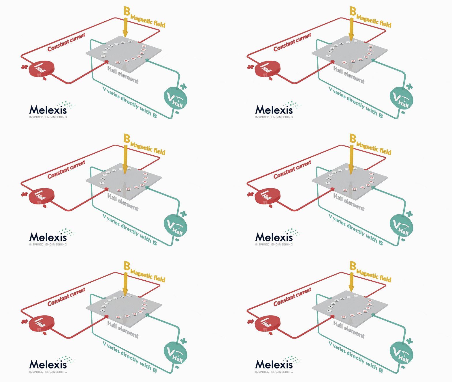
The Hall-effect principle is named for physicist Edwin Hall. In 1879 he discovered that when a conductor or semiconductor with current flowing in one direction was introduced perpendicular to a magnetic field a voltage could be measured at right angles to the current path. The common analogy popular at the time of Hall's discovery was of electric current in a wire to a flowing liquid in a pipe. Hall's theory equated the magnetic force on the current resulting in a crowding to one side of the "pipe" or wire. Electromagnetic field theory has allowed a more refined interpretation of the physics responsible for the Hall effect.
It is well established that the Hall-effect results from the interaction of charged particles, like electrons, in response to electric and magnetic fields. An excellent, detailed but highly readable explanation can be found in "The Hall Effect Sensors; Theory and Applications" by Ed Ramsden. And also on Wikipedia.
The initial use of this discovery was for the classification of chemical samples. The development of indium arsenide semiconductor compounds in the 1950's led to the first useful Hall-effect magnetic instruments. Hall effect sensors allowed the measurement of DC or static magnetic fields without requiring motion of the sensor. In the 1960's the popularization of silicon semiconductors led to the first combinations of Hall elements and integrated amplifiers. This resulted in the now classic digital output Hall switch.
The continuing evolution of Hall transducer technology saw a progression from single element devices to dual orthogonally arranged elements. This was done to minimize offsets at the Hall voltage terminals.
The next progression brought on the quadratic or four element transducers. These used four elements orthogonally arranged in a bridge configuration. All of the silicon sensors of this era were built from bipolar junction semiconductor processes.
A switch to CMOS processes allowed the implementation of chopper stabilization to the amplifier portion of the circuit. This helped reduce errors by reducing the input offset errors at the op amp. All errors in the non chopper stabilized circuit result in errors of switch point threshold for the digital type sensors or offset and gain errors in the linear output sensors.
The current generation of CMOS Hall sensors also include a scheme that actively switches the direction of current through the Hall elements. This scheme eliminates the offset errors typical of semiconductor Hall elements. It also actively compensates for temperature and strain induced offset errors. The overall effect of active plate switching and chopper stabilization yields Hall effect sensors with an order of magnitude improvement in drift of switch points or gain and offset errors.

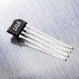
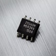
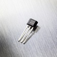
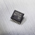
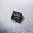
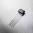
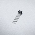
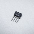
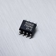
Melexis uses the CMOS process exclusively, for best performance and smallest chip size. The current developments in Hall effect sensor technology can be credited mostly to the integration of sophisticated signal conditioning circuits to the Hall IC.
Melexis introduced the world's first programmable linear Hall IC. It enables field programmable functional characteristics like gain, offset, temperature coefficient of gain (to compensate different magnetic materials thermal dependencies). The newest Hall ICs have integrated microcontroller cores to make an even "smarter" sensor with ROM programmable algorithms for complex signal processing in real time.
Example of how Melexis use Hall-effect
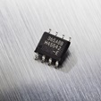
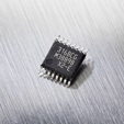
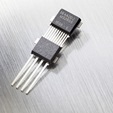
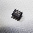
Melexis products using Hall-effect
Related products
Contact
- Environment
- General
- Investor relations
- Offices and locations
- Press
- Representatives and distributors
- Sales

